Embedded Development Board Learning
How to Control a HUB75 LED Matrix P5 with STM32 and DMA
Date: agosto 17, 2025
Author: Guillermo Garcia
Categories: Embedded C programming / STM32 Tags:
In this article, we’ll cover everything you need to understand and control the HUB75 LED matrix P5 with STM32 microcontrollers. We’ll also see how to use it with DMA.
Table of Contents
About RGB Matrix Panels
I’d never worked with this type of RGB display before. At first, I wondered how difficult it is to control these types of displays if you just turn on a single LED. But when I started working, I realized the possibilities are vast. Each LED within the matrix can take on a different color for a set amount of time. Now imagine that in a 32 x 64 HUB75 LED matrix P5.
That’s where things start to get interesting, so in this article, we’ll analyze all the details to understand how these LED matrix panels work.
Panel LED P5 32×64
Let’s present the panel we worked with for this article, HUB75 LED matrix P5 it is a 32×64 pixel matrix that is usually identified as P5. We see the panel in the following image.

Each RGB LED represents a point in the matrix that we will call a pixel and they are organized by rows and columns in this way we can address each pixel in the matrix.
Let’s look at the back of the Panel where we find a series of connectors, the HUB75 connectors.
HUB75
What is a HUB75? One thing I found was that this type of connector isn’t very standardized, but it is common to find it on this type of panel. We can see three connectors on the back of the matrix: two of them are the HUB75 connector interfaces, and in the center is the power connector.

The RGB Matrix Panel is made up of standard tri-color LED chips. Each color of each LED is controlled by a bit in a shift register. All the shift registers are daisy-chained together, allowing all the LEDs to be controlled by synchronizing the high or low bits for the red, green, and blue LEDs individually. We’ll look at this later before we break down the HUB75 connector.
The HUB75 connector for connecting this type of display has the following pin distribution:

The connector splits the colors into two sections R1,G1,B1 and R2,G2,B2 instead of going through 32 lines you have two pixel channels RGB1 and RGB2 each update draws two lines at a time leaving you only 16 lines to address. Addressing is done via inputs A, B, C and D.
Additionally, we have a CLK signal that is used to shift data into the shift register chain and a LATCH signal to move the shifted data to the output (pixels).
Finally, OE, the output enable, is used as a global output switch to turn all pixels on the display on and off. This can also be modulated to control the intensity of the output brightness. These displays, given enough current, can be quite bright, so by limiting the time the output is enabled (OE is usually active at low), the brightness and current draw can be adjusted.

scan pattern
Now that we know the signals present in the HUB75 we can understand how each pixel is controlled, the scanning pattern is the way in which we can control each pixel within the matrix since we have two channels R1 and R2 the matrix is divided into two sections.
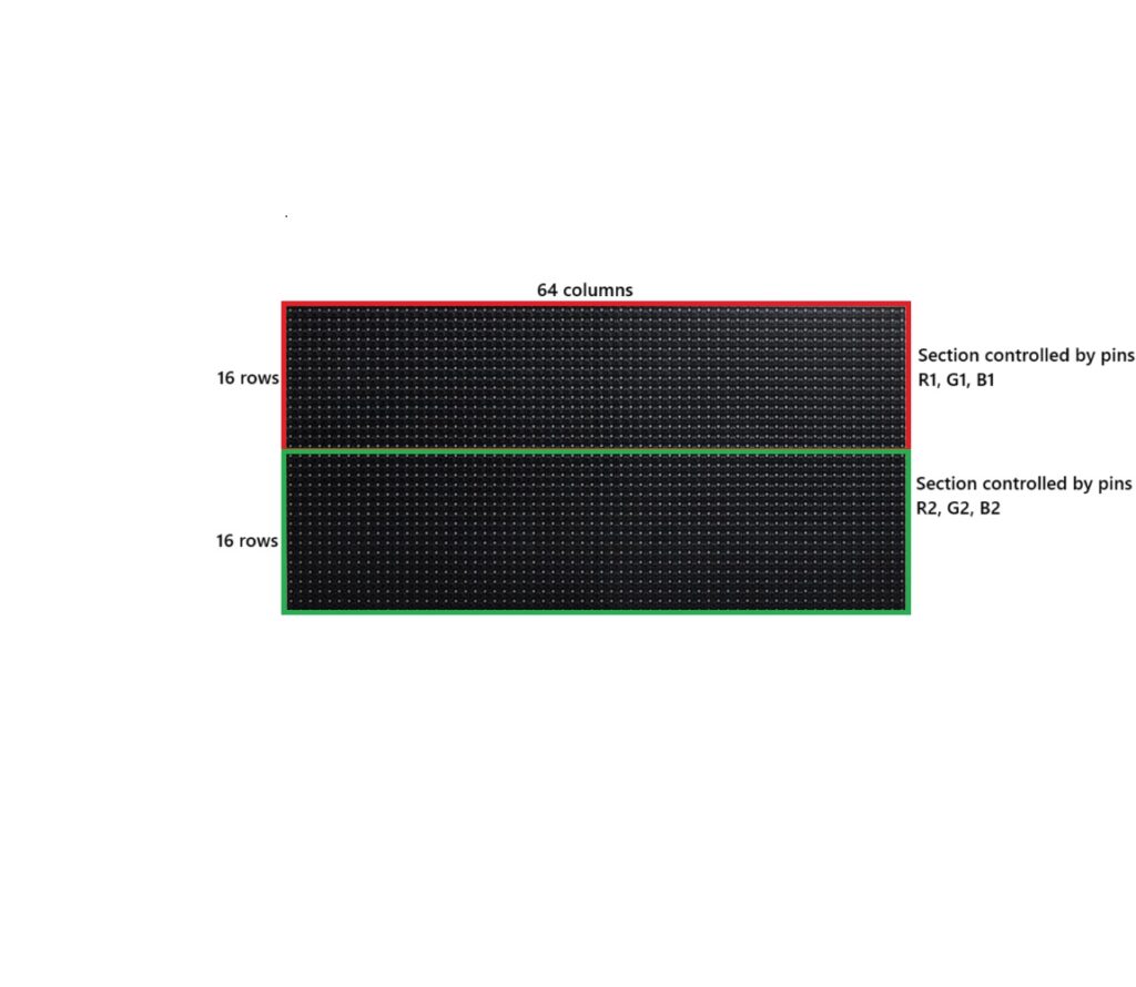
The screen is divided into two horizontal halves:
- Upper half → uses data lines R1, G1, B1
- Lower half → uses data lines R2, G2, B2
When you activate an address (A, B, C, D), the panel’s internal controller turns on one line of the upper half and the corresponding one of the lower half at the same time.
Let’s keep the following idea in mind before continuing, we can conclude that we have a 1/16 scan pattern, this means that only 1/16 of the total rows are lit at a time in this case 2 rows of LEDs because there are 2 halves, top and bottom.
shift registers
The panels have shift registers and multiplexers. For the model we’re using, we’ll have 64 shift registers for the 64 columns.
Each pixel is an RGB pixel, which means that 3 bits are generated for each pixel: one to indicate whether the red LED should be on, one for the green, and one for the blue, so we need to enter 64 RGB values in each row.
This is where the addresses become relevant, since with the combination of A, B, C, and D, we can choose which pair of rows to turn on.
| A | B | C | D | Rows lit (top, bottom) |
| 0 | 0 | 0 | 0 | 0 y 16 |
| 1 | 0 | 0 | 0 | 1 y 17 |
| 0 | 1 | 0 | 0 | 2 y 18 |
| 1 | 1 | 0 | 0 | 3 y 19 |
| 0 | 0 | 1 | 0 | 4 y 20 |
| 1 | 0 | 1 | 0 | 5 y 21 |
| 0 | 1 | 1 | 0 | 6 y 22 |
| 1 | 1 | 1 | 0 | 7 y 23 |
| 0 | 0 | 0 | 1 | 8 y 24 |
| 1 | 0 | 0 | 1 | 9 y 25 |
| 0 | 1 | 0 | 1 | 10 y 26 |
| 1 | 1 | 0 | 1 | 11 y 27 |
| 0 | 0 | 1 | 1 | 12 y 28 |
| 1 | 0 | 1 | 1 | 13 y 29 |
| 0 | 1 | 1 | 1 | 14 y 30 |
| 1 | 1 | 1 | 1 | 15 y 31 |
About STM32 Boart
For this article, we’ll be using the NUCLEO-H723ZG development board, which has sufficient resources to control a panel with relative ease and also integrates a DMA and TIMER peripheral.
The reason for choosing STM32 microcontrollers is that they can emulate parallel synchronous communication through the GPIO interface, using the integrated DMA protocol. The transmitted frame consists of up to 16 bits of data and a synchronous data clock. Transmission requires the use of timers to generate the data clock and control the transmission duration. We’ll see how this works in the rest of this article.
GPIO + DMA parallel port
This feature will allow us to control the data outputs without intervention from the CPU through a timer we can control the firing frequency for the DMA and move data from the memory to the peripheral which is GPIOS a series of output ports where this data will be represented by the state of dico pins, this can be seen in the following image.
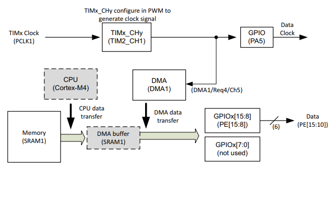
Simply if we have the value 0x8 in memory and we move this to the parallel port, the pins chosen as output will take the state 00100, for example the series of pins of port E from 10 to 15 are the parallel output port PE[15:10] and we will only have a logical 1 value on the corresponding pin.
Configure HUB75 data port
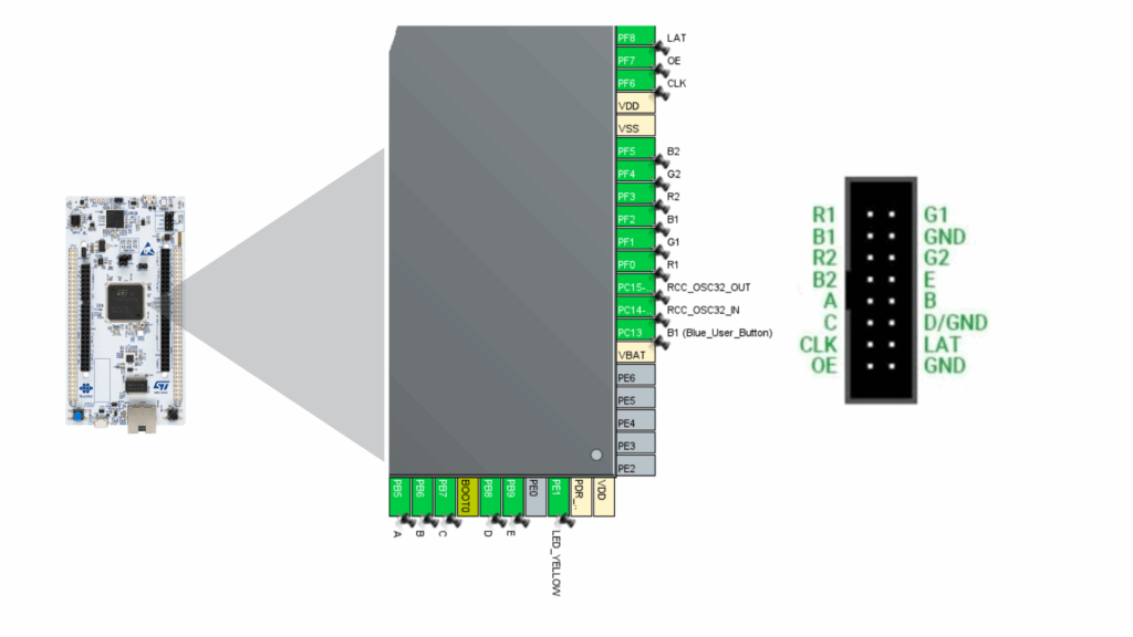
Let’s configure the data output port required for HUB75 we need 6 output pins we will choose port PF0 to PF5, we configure the ports as high speed.

Configure HUB75 control port
For the control signals we will configure port PB5 to PB9 as high speed output, we will control these signals in the code.

The pin assignment is as shown in the image below.
Configure CLK and EO Signal
For the CLK signal, we’ll configure a TIM16 timer to generate a PWM signal that can be routed to pin PF6.
TIMER16 will initiate the DMA.

We will handle the OE signal in the code by managing the state of that pin.
Coding and viewing signals
We create a function where we initiate the first data transmission over the DMA and reserve a memory space to store the data.
static uint32_t DATA_DMA[64 * 16];

void HUB75_StartScandDMA(void)
{
	//! Turn off output
    HAL_GPIO_WritePin(OE_GPIO_Port, OE_Pin, GPIO_PIN_SET);

    HAL_GPIO_WritePin(A_GPIO_Port, A_Pin, (current_row & 0x01) ? GPIO_PIN_SET : GPIO_PIN_RESET);
    HAL_GPIO_WritePin(B_GPIO_Port, B_Pin, (current_row & 0x02) ? GPIO_PIN_SET : GPIO_PIN_RESET);
    HAL_GPIO_WritePin(C_GPIO_Port, C_Pin, (current_row & 0x04) ? GPIO_PIN_SET : GPIO_PIN_RESET);
    HAL_GPIO_WritePin(D_GPIO_Port, D_Pin, (current_row & 0x08) ? GPIO_PIN_SET : GPIO_PIN_RESET);

    //! The DMA will be responsible for outputting data and writing to GPIOF->ODR every CLK cycle
    HAL_DMA_Start_IT(&hdma_tim16_ch1,
                  (uint32_t)&DATA_DMA[current_row * 64],
                  (uint32_t)&GPIOF->ODR,
				  64);

    //! Activate trigger from PWM
    __HAL_TIM_ENABLE_DMA(&htim16, TIM_DMA_CC1);

    SCB_CleanInvalidateDCache();

    //! Start CLK (PWM)
    HAL_TIM_PWM_Start(&htim16, TIM_CHANNEL_1);
}
Once we start timer16, it will continue performing DMA transmissions. When the transmission is finished, we will have an interruption for the DMA, and then we will again call the HUB75_StartScandDMA() function.
void DMA1_Stream0_IRQHandler(void)
{
  /* USER CODE BEGIN DMA1_Stream0_IRQn 0 */

  /* USER CODE END DMA1_Stream0_IRQn 0 */
  HAL_DMA_IRQHandler(&hdma_tim16_ch1);
  /* USER CODE BEGIN DMA1_Stream0_IRQn 1 */
  HUB75_DMA_ISR_Callback();
  /* USER CODE END DMA1_Stream0_IRQn 1 */
}
The HUB75_DMA_ISR_Callback() function checks the LAT signal and activates the OE signal, it also switches to the next control address to restart the cycle by calling HUB75_StartScandDMA() again to start the next DMA transmission.
void HUB75_DMA_ISR_Callback(void)
{
    HAL_TIM_PWM_Stop(&htim16, TIM_CHANNEL_1);
    __HAL_TIM_DISABLE_DMA(&htim16, TIM_DMA_CC1);

    //! Display data in the matrix
    HAL_GPIO_WritePin(LAT_GPIO_Port, LAT_Pin, GPIO_PIN_SET);
    HAL_GPIO_WritePin(LAT_GPIO_Port, LAT_Pin, GPIO_PIN_RESET);

    //! Activate output
    HAL_GPIO_WritePin(OE_GPIO_Port, OE_Pin, GPIO_PIN_RESET);

    current_row = (current_row + 1) % 16;

    //! Continue with next row
    HUB75_StartScandDMA();
}
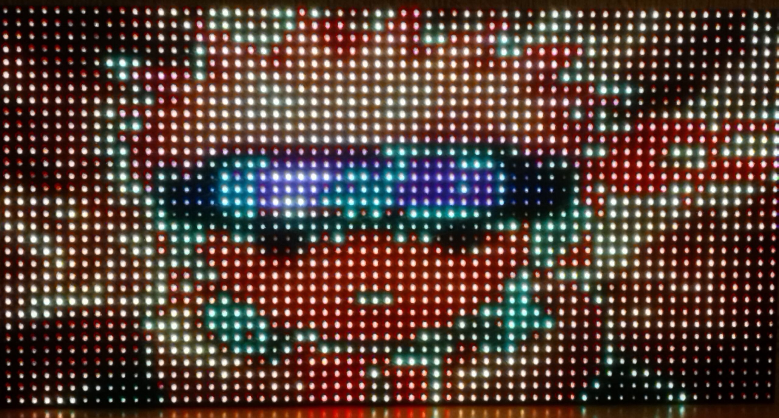
LED On
Let’s test how the control is performed if we want to turn on the red LED of the coordinate 0,0 we place the value 0x09 -> 001001 in the memory.

We put this in the memory section we reserved DATA_DMA.

Signals
We connect the logic analyzer to see how the signals are being generated. We can see that the 0x9 are transmitted in the set of outputs R1, G1, B1, R2, G2, B2.

The series of control signals A,B,C,D we see that it moves from 0000 to 1111.
Physically we see that the LEDs at the coordinate 0,0 we see the LEDs lit in red.

Typically this is how signals from a HUB75 LED matrix P5 port are generated.
Comments... a comment
Noel Dom dice:
crack
Deja una respuesta